


IBM this week at an IEEE CAS/EDS AI Compute Symposium advanced an effort to improve the efficiency of systems by a factor of a thousand by 2029. It aims to accomplish this by giving developers access to an open-source Analog Hardware Acceleration Kit written in Python. The kit enables them to begin testing an approach to in-memory computing that will run neural networking algorithms much faster than any existing processor.
See also: Hardware Acceleration Drives Continuous Intelligence
The processor IBM is developing achieves that goal by combining compute and memory in a single device to overcome what is known as the Von Neumann bottleneck. On conventional systems, computation and memory are segregated in different locations. Information is moved back and forth between computation and memory units every time an operation is performed.
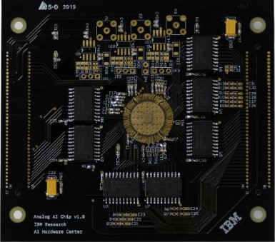
IBM researchers have already developed a 200-millimeter square chip that overcomes this bottleneck by processing and storing data in memory, says Mukesh Khare, vice president of systems research for IBM.
The two main components of the Analog Hardware Acceleration Kit is an instance of PyTorch, which is an instance of an open-source machine learning library based on the Torch library, and an analog devices simulator. IBM is looking to work closely with software developers that will commit to building software in parallel with IBM’s ongoing processor research, says Mukesh Khare, Vice President, IBM Research.
As part of that effort, IBM this week revealed that Red Hat, which it acquired last year, is now optimizing its OpenShift application development and deployment platform based on Kubernetes for this processor project. The goal is to narrow the gap between when the processor is completed and application software that takes advantage of it is available, notes Khare.
“The idea is to develop a full stack approach,” says Khare. “We want software development to be enabled in parallel.”
IBM also announced that Synopsys, a provider of electronic design automation (EDA) software and emulation and prototyping solutions, has become the lead (EDA) partner for IBM’s AI Hardware Center in Albany. N.Y. Synopsys also develops IP blocks for use in the high-performance silicon chips along with other software tools for building artificial intelligence (AI) applications.
Finally, IBM this week also revealed it is investing in a new cleanroom facility on the campus of, SUNY-Poly, in Albany, N.Y. to advance packaging, also known as heterogeneous integration, to improve memory proximity and interconnect capabilities. The goal is to ensure as compute cores are developed that memory bandwidth increases in tandem. Those research efforts are focused on fine pitch laminate technology, implementation of silicon bridges embedded in the laminate to provide fine pitch interconnect between AI chips; and full 3D integration through the stacking of memory with the AI chip.
Ultimately, the processor IBM is developing will enable AI applications based on neural networks, also known as deep learning algorithms, to respond to events much faster by storing data in memory in a way that makes it possible to process simple weight calculations much faster, says Khare. AI inference engines deployed on edge computing platforms will especially benefit, he adds.
It may be a while before the benefits of this IBM research project are fully realized. In the meantime, however, it’s clear that as far as AI applications are concerned the IT industry as a whole is still very much at the beginning of what promises to a journey where many existing assumptions concerning what is and what’s not possible may not hold.